
How to Reduce EMI/EMC Noise in Power Electronics?
A power converter design that works flawlessly in the lab may fail certification due to excessive conducted or radiated emissions in the EMC test chamber, which is one of the most common problems faced by power electronics engineers. EMI noise reduction is an indispensable part of switch-mode power supplies; because modern converters operating with high dV/dt and di/dt values inherently produce wide-band electromagnetic interference. In this article, we discuss the origin of EMI/EMC noise, how it propagates, and how it can be suppressed with a layered approach from an engineering perspective. You will find applicable techniques from proper filter selection to board layout, grounding to shielding, and EMI filter solutions to support them.
What is EMI and EMC? Basic Concepts
EMI (Electromagnetic Interference / electromagnetic interference), is the electromagnetic energy undesirably produced by an electronic circuit and potentially disrupting the operation of other circuits. EMC (Electromagnetic Compatibility / electromagnetic compatibility) refers to a device's ability to operate both without emitting noise above acceptable levels and with immunity to external interference. In short, EMI is a problem, while EMC is the name of the compatibility goal..
EMC is examined in two main axes: emission (the noise emitted by the device) and immunity (the device's resistance to external noise). Emissions are also divided into two:
- Conducted emission: This is usually noise transmitted through power and signal cables, in the range of 150 kHz to 30 MHz. This is the primary target of EMI filters.
- Radiated emission: This is the energy emitted by circuit traces and cables, acting as antennas, into space, typically above 30 MHz. The solution is more related to layout, shielding, and board design.
Standards such as CISPR 11, CISPR 32 (EN 55032), and CISPR 16 for industrial equipment specify the limits that apply in each frequency band. Knowing the target class (Class A for industrial, Class B for residential environments) from the outset is the first step in selecting the correct clamping strategy.
Where Does EMI Noise in Power Electronics Come From?
In switch-mode power converters, the main source of noise is the rapid switching of MOSFETs or IGBTs, which occurs tens of thousands to millions of times per second. These switching events generate two types of noise:
- Differential mode (DM) noise: Noise associated with the current cycle between the phase and neutral (or V+ and V−) lines. It is typically present at lower frequencies and is caused by the pulsating nature of the input current.
- Common mode (CM) noise: Noise flowing in the same direction on both power lines, completing the return path through the ground/chassis. It is formed over parasitic capacitors between high dV/dt points (e.g., MOSFET drains) and the chassis, and is prevalent at high frequencies. CM noise is the most troublesome component in EMC testing.
Distinguishing between these two modes is the key to selecting the correct solution: DM noise is suppressed with X capacitors and differential inductors, while CM noise is suppressed with a common-mode choke and Y capacitors. A pre-measurement using a LISN (Line Impedance Stabilization Network) and a spectrum analyzer shows in which mode and at which frequency the noise is concentrated, which is much faster than trial-and-error component testing.
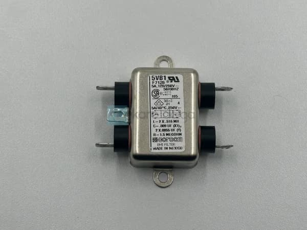
 The line filter connected to the network input suppresses the transmitted EMI noise at its source. Example: Corcom 5VB1 EMI Filter.
How to Reduce EMI Noise? Layered Approach
In EMI reduction, there is no single magic component; the most effective result is achieved by applying a three-layered strategy of reducing noise at the source, breaking the path and protecting the victim. The following ranking starts with the steps that provide the most gain in practice.
1. Reduction at the Source: Softening Switching Behavior
Reducing noise before it spreads allows subsequent layers to relax. By optimizing the gate capacitance to keep switching edges from switching too quickly, snubber (RC) circuits and soft switching (ZVS/ZCS) topologies, dV/dt and ringout are reduced. Here, balance is important: very slow switching reduces EMI but reduces efficiency and increases heat.
2. Cutting the Path: EMI Filters and Board Layout
The most powerful tool for conducted noise is an EMI filter placed on the power input. A typical line filter consists of a common mode choke, X capacitors (line-to-line, DM suppression), and Y capacitors (line-to-ground, CM suppression). It is critical to connect the filter to the converter's input terminal as closely as possible, with short and direct paths, to prevent the input and output traces from coupling to each other.
On the board (PCB) side, reducing the area of high di/dt current loops (e.g., placing the input capacitor very close to the switch), using a solid reference/ground plane, and keeping the noisy switching node (switch node) small, directly reduces the radiated emission.
3. Victim Protection: Shielding and Grounding
For residual radiated energy, conductive enclosures (frame shielding), braided shielding on cables, and ferrite beads are used. The grounding architecture (single point/multiple point/hybrid) should be selected according to the frequency; single point grounding prevents ground noise loops at low frequencies, while multiple point bonding reduces impedance at high frequencies.
How to Choose the Right EMI Filter?
Filter selection requires more than just looking at the current value. The following table summarizes the key parameters to consider in the selection and their practical meanings:
| Parameters | Why is it important? | Practical Tip |
|---|---|---|
| Nominal current/voltage | The load that the filter can continuously carry; overheating and saturation result | Leave a margin above the maximum continuous current |
| The insertion loss curve | Shows how much attenuation is provided at which frequency | Match the curve with your problem frequency band |
| CM/DM distinction | Which mode of filter topology is more dominant | Select a filter that matches your dominant noise mode |
| Leakage current (Y-cap source) | Safety and leakage current relay compliance | Choose low-leakage type for medical/human contact applications |
| Mounting type and temperature | Mechanical and thermal compatibility | For chassis-mounted types, the ground connection must be clean |
Different solutions are highlighted depending on the application profile. In industrial equipment and drives, noise filters such as the Delta Electronics FL75L05-A or the higher-current variant, the Delta Electronics FL75L10-A are commonly considered. For general-purpose network input suppression, LCR Electronics LCR 091.02001.00 type modules are preferred for compact power supply designs, while surface-mount solutions are preferred for card-top solutions. You can find brand-specific options on the Delta Electronics and LCR Electronics You can take a look at our pages.
 Chassis-mounted line filters suppress radiated emissions over a wide bandwidth. Example: Delta Electronics FL75L05-A.
Module Level EMI Suppression: Board Level Filters
Not all noise problems are solved at the power entry. In high-density power distribution architectures, using board-level EMI filters at the output or input of each DC-DC point, cuts the noise close to the source, before it spreads throughout the system. This approach is particularly effective in multi-point of load (PoL) designs, preventing noise from coupling to other modules through the common DC bar.
In this class Picor 9LZ-01 (QPI-9LZ-01) and complementary output filter Picor QPO-1LZ such as active/passive module solutions, are designed to provide high suppression in the compact card area. When selecting these types of modules, filtering the input and output sides separately breaks the noise circulation through feedback. For detailed options Picor and line-type solutions Corcom brands can be reviewed.
 Card edge filter modules cut off the noise on the input side of DC-DC converters close to the source. Example: Picor 9LZ-01 (QPI-9LZ-01).
A good rule of thumb is to distribute the suppression rather than try to fix the system with a single large network filter: while the input filter assumes the bulk of the broadband fundamental suppression, each noisy module has its own local filter that attenuates the high-frequency CM component at its source. This hierarchical approach reduces the size of the filter components and facilitates detection by preventing a module failure from affecting the entire system.
Frequently Asked Questions
What is the difference between common mode and differential mode noise?
Differential mode noise flows between the two power lines and is related to the current loop of the circuit; it is suppressed by X capacitors and differential inductors. Common mode noise, on the other hand, flows in the same direction on both lines and returns to ground/chassis, and is caused by high-frequency and parasitic capacitances; it is suppressed by the common mode coil and Y capacitors.
Where should I place the EMI filter in the circuit?
The filter should be placed as close as possible to the power terminal at the input point between the noise source and the outside world. The input and output traces of the filter should be kept separate, and the ground connection should be short and have low impedance; otherwise, the filtered line will couple with the unfiltered line, reducing performance.
Does a ferrite bead solve the EMI problem by itself?
Ferrite beads are a useful complement to high-frequency noise, but they are not sufficient on their own. By offering impedance over a specific frequency range, they reduce CM noise on the cable in particular; however, they must be used in conjunction with a filter, layout, and shielding for a broad-band EMC solution.
How can I perform preliminary checks before entering EMC testing?
Performing a desktop pre-measurement with a LISN and spectrum analyzer (or a nearby field probe) will show at which frequency and mode the limit is exceeded. This allows you to make targeted improvements to filter values, layout, and shielding before entering formal testing, significantly reducing certification risk and cost.
Summary and Next Step
Reducing EMI/EMC noise relies on a holistic engineering approach, consisting of softening at the source, proper filtering and routing, and shielding/grounding in the final layer, rather than a single component. Diagnosing noise as differential and common mode first, then selecting an EMI filter suitable for the problematic frequency band is the key to passing certification in the first attempt for most designs. You can review the line or board-level filter options suitable for the power, current, and target standard of your project from the Kare Dalga catalog, and you can get a quote from us for the model that suits your needs.